|
Home |
|
Contact |
|
Service List |
|
Project List |
|
Publications |
|
Other Material |
|
Related Links |
|
Home | Contact | Service List | Project List | Publications | Other Material | Related Links |
|
Some examples of recent projects, activities, and interests are outlined below. |
|
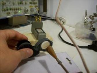
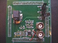
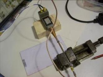
The picture on the top left shows a demonstrator board constructed for a PLL fundamentals course. The picture on the bottom left shows a sample of the corresponding course documentation. The diagram is used to explain a particular measurement setup. The material was initially intended for “at -presence” learning. However, the material also includes a comprehensive set of simulation files and experiments that the student can use to get up to speed prior to attending the lab sessions. The board and simulation files allow the student to carry out basic functional, step response, VCO gain, and phase transfer function measurements. In addition, principles of frequency and other measurements are introduced. Further motivations behind the material are outlined in a corresponding paper. A subset of the course material was also modified to work with a remote access laboratory at Limerick University (see publications page). This version allowed experiments to be carried out remotely via an internet link. Various modifications and additions to the material are planned. In addition, further courses of this type are being developed. If you are interested in the material please contact me. |
|
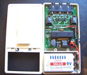
The picture to the left shows a PIC based “generic” analogue I/O module. The unit uses the PIC’s onboard A/D for analogue data acquisition and two 256 position digital potentiometers for coarse voltage generation. The reverse side has a few leds and tact switches for status and control. Also, there is an EEPROM area for storage of values. The right hand side of the board shows a sil connector. This connector can be used to connect to an RS232 level shifter to allow PC communications. The same connector has also been used with an RF PIC and USB interface. The module was initially intended to be used in conjunction with a MAX038 function generator IC to allow control of the frequency adjust input on the MAX038. The specific purpose of this function was to allow a frequency modulated input to be applied at the reference input of the PLL measurement demonstrator board (see above). As time has progressed I have added some other functions that are of use to me. |
|
As well as refinement and additions to the activities outlined above, I also have a number of other ongoing projects, some of which I am carrying out for my own interest. Key areas relate to development of DDS and PLL based synthesizers and data acquisition systems hardware. In addition, I have interests in sigma delta converters for communications applications. I am also developing further simulation based training material based upon the principals of the PLL course. In addition, I have professional and personal interests in electronics and technology related to renewable energy applications. Further information for these activities can be found at www.ecopivotal.co.uk The site will be updated as appropriate. |
|
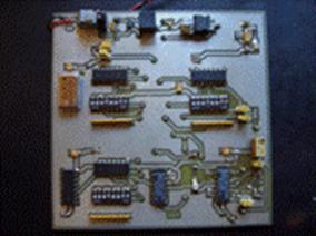
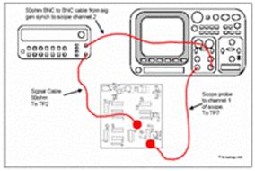
Most of these boards are experimental prototypes which I have used to carry out basic experiments relating to some PLL BIST / DFT test techniques. The board uses a relatively low speed true charge-pump version of the 74HCT4046 Pll chip. Im currently planning to upgrade this version with an off-chip higher frequency oscillator and perhaps some external high-speed logic. The second picture shows a PLL test board piggy-backed onto a Spartan II development board. This arrangement was used in for test evaluation in a similar manner to that of the first board, however, it was targeted to higher-frequency PLL’s . I’m also planning to proceed with the work in this area and look at refining the solutions and develop other techniques. The third picture shows an initial piggy back board that will be used to look at supply noise injection. Two key publications that I am eager to progress are shown here. If you are interested in some of this work please contact me. Some more details of the setups can be found in various publications.
|
|
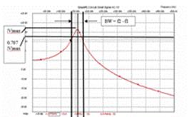
I have a variety of electronic spice circuit simulation files and corresponding course tutorial notes. The material covers basic circuit concepts, high-pass, low pass, RLC circuits , and various other op-amp, filter and transistor circuits. This material was initially developed to support basic undergraduate electronics lectures. However, the material includes sufficient background detail relating to the circuits to allow it to be delivered in a self contained manner. I also have a selection of more advanced modules that introduce basic MOSFET operation and techniques. In the past I have used the simulation files in conjunction with corresponding lab sessions based upon real hardware. I found that this methodology was particularly useful for emphasizing the difference between actual measurements and simulations. All simulations were developed for the B2SPICE simulator. However, they are easily adapted to other spice based simulators. The pictures to the right illustrate a MOSFET curve tracing simulation plot (top), an RLC circuit plot (middle), and a simple sample and hold circuit (bottom). I can deliver courses based on part or all of the material. I can also develop new material based upon customers requirements.
|
|
Simulation and hardware demonstrator for a PLL fundamentals course |
|
PLL test development boards and research |
|
Other ongoing projects |
|
Handheld low-speed analogue I/O /Data logger module module |
|
Electronic circuit simulation modules |
|
Project List |

|
For more information: |
|
E-mail: martin_at_mjb-rfelectronics-synthesis_dot_com |
|
1 kW E-Class Amplifier module (RF source) |
|
The picture to the left shows a 1kW 13.56 MHz E-Class amplifier (RF-source) module that was designed and built for a client. The source has high efficiency, measured at typically greater than 87%. In addition, it has a small area (200 mm x 90 mm). The board was constructed as a 2-layer FR4 board. Various monitoring points were included and coupled to safety shutdown mechanisms (see below). The grey block at the top of the module is a plug in RF sensor linked to the external monitoring circuitry. |
|
RF source safety shutdown circuit |
|
The module on the right is a prototype unit that isolates the main supply to an RF source in the event of an error condition. The unit was used with the RF source shown above. The supply line switching capabilities are 300 V @ 7A. The module monitors heating temperature, supply current and drain voltage . It automatically isolates the amplifier supply if an “over “ condition occurs. Extra inputs are included for monitoring of other parameters such as VSWR. |
|
16-bit 80 Ms/s A/D board |
|
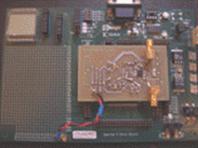
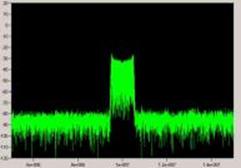
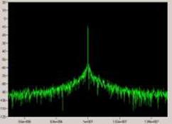
The picture to the left shows a prototype 80 Ms/s, 16-bit DAQ board that I recently designed and constructed. The board contains a 64K x 18-bit FIFO, a Cypress EZ-USB micro as a high-speed USB interface. (This uses the BITWISE firmware), and an Analog devices AD9446 ADC. The board is 6-layer and was fabricated by PCB-POOL.
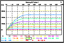
The topmost plot shows the output from the board with the following input signal. FSK: Deviation 500 kHz, Modulation 5 kHz
The bottom plot shows the output from the board with the following input signal. -10dBm, 10 MHz sine signal from a HP 33120A signal generator displayed over 64K samples. (BW: 40 MHz, 10 MHz, 1 MHz). |
|
CPLD and PLL development board |
|
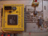
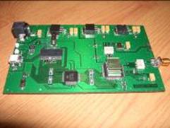
The picture to the left shows a CPLD and PLL development board. The board is 4-layer and includes a USB interface a Xilinx CPLD an onboard PLL and a DDS chip. The board was initially developed for training purposes as an extension to the PLL course shown on this site. |
|
MJBRF-Electronics Dr. Martin John Burbidge |
|
Electronics and RF, research, development and prototyping. |
|
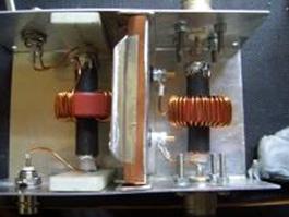
1.5 kW capable H.F. Directional coupler |
|
The picture to the left shows a 1.5 kW capable directional coupler. The frequency range is approximately 3-30 MHz and the coupling ratio is approximately 30 dB. The unit is used to monitor the forward and reflected power and phase difference in conjunction with the phase magnitude detector outlined in the next section. Suitable first load resistors for the coupled ports, are placed on the phase magnitude detector PCB. |
|
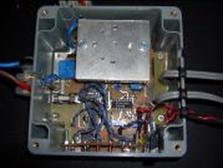
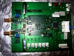
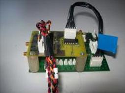
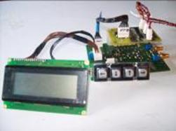
Phase magnitude tuner board—controller tuning unit |
|
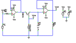
The pictures to the right show a phase and magnitude detector and controller system board. The board was developed to link the E-class RF source to the RF source safety shutdown circuit, a load matching unit (“antenna tuning unit”), and an adjustable switched mode power supply. The unit was connected between the tuning unit and the RF source on the main RF line, via the directional coupler. The units functions were to control the power of the RF source via the SMPS, monitor the magnitude and phase (basically VSWR + phase information) and adjust the tuner (via motors) accordingly. The tuning unit was a motor controlled custom transformer coupled capacitive tuning unit . The unit also interfaced to the safety shutdown circuit (outlined above) to provide an “over VSWR” shutdown function. The back-end monitoring circuits of the phasemag unit have also been used with success (after some tweaking) up to 2GHz, however in this case, different PCB / Microstrip, and off-the-shelf directional couplers were used. The pictures are as follows: Top: main board, sma connectors to directional coupler on LHS. Limit switch inputs from tuner at bottom. Motor driver connector bottom right-hand corner. Middle: main board with one motor driver board connected. Bottom: main board connected to lcd display and keypad. |
|
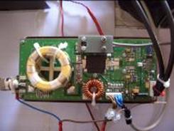
1.3 kW 30-285 Vdc Half-Bridge switched-mode power supply (prototype-next phase) |
|
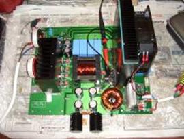
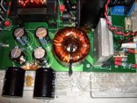
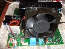
The pictures to the left show a voltage mode controlled half-bridge switched-mode power supply that I designed to supply the DC requirements of various E-class and C-class RF sources. The supply was used with the E-class source outlined above. The basic topology consists of a 1.5 kW PFC circuit followed by a half bridge voltage-mode-control switching converter. Drives to the primary side of the switching converter are transformer isolated. The DC output of the PSU can be adjusted from 30 to 285Vand can source about 4.5A. Adjustment of output voltage is jumper selectable so that it can be altered by a manual trimmer or a digital pot. If the digital pot is selected the output can be adjusted manually by use of tact switches or automatically via the phase-mag unit outlined above. In the pictures some of the cooling fans were initially “hung” from the heat-sinks. In later versions they were incorporated into a custom enclosure. One problem in initial testing was overvoltage spikes on the PFC low voltage supply, this would cause the PFC boost transistor to fail catastrophically and dramatically. Unfortunately I don't have pictures of this but the MOS transistor was unrecognizable. Prior to using this unit, I used an isolation transformer, a 10A variac with a capacitive output filter and rectification for test of high-voltage supply RF sources. I still use this supply for initial testing. |
|
E-class sources and supporting circuitry—Further information. Further information and pictures relating to the E-class amplifier and supporting circuitry shown above, can be found here If you have any requirements for circuits and systems relating to the ones highlighted, please do not hesitate to contact me. |
|
60 GHz mmwave harmonic multiplier — weak signal source — Very preliminary experiments |
|
The pictures to the right show an experimental harmonic multiplier using an Avago 10-14 GHz anti-parallel Schottky mixer diode. The diode multiplier was fed via a HP8350b swept signal source with an 8-20GHz 100mW plugin. The input signal frequency was approximately 12 GHz. The output signal was monitored using a HP8569b spectrum analyzer with an external harmonic mixer. Monitored signal levels (not calibrated) were in the region of –55dBm at 60 GHz. At the moment it is more important for me to have a reference level that I can make relative measurements against. This work is ongoing. Some more pictures on construction and some rough videos showing operation are here. |
|
60 GHz through a looking glass — using a dielectric lens at 60 GHz to increase antenna gain |
|
The pictures to the left show the experimental harmonic multiplier (outlined above), used with a couple of cheap acrylic magnifying glasses placed between source and load. I wanted to do a very quick observational test to see if this would change the gain at 60GHz. Anyway, using this very rough setup, it seemed quite easy to increase the gain by 10dB. Although it was quite difficult to align the lenses. I'm currently having some custom lenses cast and polished, and making a custom test rig to carry out further experiments. This work is ongoing. A rough video showing operation and increase of signal gain is shown here.
|